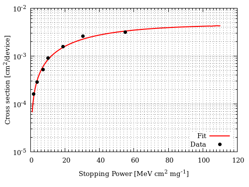
Cookie Policy

Welcome to SR-NIEL. This site uses cookies. Read our policy.

Learn more
Logo HelMod small

SR-NIEL – 7

Screened Relativistic (SR) Treatment for NIEL Dose

Nuclear and Electronic Stopping Power Calculator

(version 10.16)

Proton High AMS02 small

SEE Cross Section
Minimization method
values:
(use dot "." as decimal separator)
* No errors are requested for
equally weighted data points
Stopping Power
[MeV cm2 mg-1]
Cross Section
[cm2 device-1]
* Cross Section error
[cm2 device-1]

Optionally Fixed Parameters
Saturation cross section - A: [cm2/device]
LET Threshold - x0: [MeV cm2 mg-1]
Plotted Cross Section Options
Cross section as a function of


EXAMPLE:
Copy and paste the data (without errors) here to reproduce the following example with MIGRAD+HESSE as minimization method:

and MIGRAD alone:


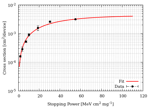
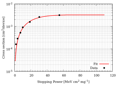
Copy and paste the data (with errors) here to reproduce the following example with MIGRAD+HESSE as minimization method.
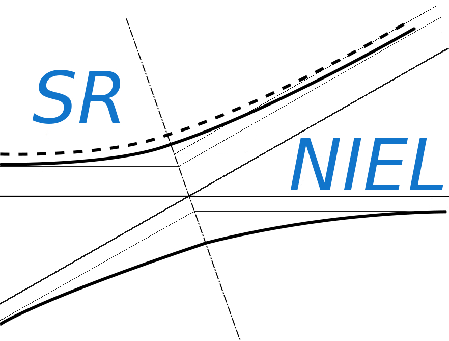
To be remarked about W0
To a first approximation, W0 can be estimated from the electron energies whose corresponding total ranges allow electrons to be fully absorbed inside the medium, i.e., such energies cannot exceed that corresponding to the maximum pathlength inside the device. For electron energies where the radiation energy-loss is not a significant part of the energy-loss process, the practical ranges of electrons in units of g/cm2 are almost independent of the atomic mass-number of traversed absorber (e.g., see Equation (1-21) in Section 1-10 of [Price (1964)] and discussion in Sect. 2.3.2 of [Leroy and Rancoita (2016)]). An example of practical range in g/cm2 of electrons is shown in Figure 9 in this webpage). The curve is obtained using Eq. (2.134) in Sect. 2.3.2 of [Leroy and Rancoita (2016)] (see also, Eq. (1-18) in Sect. 1-10 of [Price (1964)]). Furthermore, values of the CSDA ranges of electrons in materials can be obtained from ESTAR database at NIST. Practical ranges and CSDA ranges of electrons may be employed to roughly estimate the values of W0 for microelectronic devices or semiconductor detectors.

The indicated default-value of 100 keV for W0 approximately corresponds to a practical range (see webpage) of about 0.0135 g cm-2 for electrons in an absorber or in a device active-depth directly exposed to the incoming particles flux. For a correct usage of the present web calculator, the inserted value of W0 should appropriately account for absorber thickness (or device active-depth) and enviromental conditions.

NOTE:
  • The lower energy limit is 1 eV
  • W0 is set to be larger than five times the mean excitation energy of the absorber.
  • Target selection for the results obtained in the EXAMPLE section
    Selection for Fe ions in Silicon:

    Selection for Fe ions in GaAs:

    Selection for Fe ions in Water Liquid:

  • User can select the target as gas only for elemental gas targets: H, He, N, O, F, Ne, Cl, Ar, Kr, Xe, Rn.
  • FINAL REMARK:
  • Input data with a null value for the cross section are not used in the fitting procedure, but to deterrmine the minimum value of the "Stopping power (or LET) Threshold - x0"
  • In the present stopping to energy conversion, it is assumed that the current effective maximum detectable energy (W0) is correctly accounting for delta rays energy deposition (see Sect. 2.1.1.4 of Leroy and Rancoita (2016)).
  • For few compounds belonging to the ICRU list the parameters employed for the energy loss formula (including those for the densiity effect) are reported in Table II of Sternheimer et al. (1984).
  • For the conversion of the cross section as a function of the incoming particle energy, the input cross section is assumed to be provided as a function of the corresponding type of the selected energy loss (i.e., SRIM Electronic stopping power, SR-Framework Electronic stopping, SR-Framework Restricted energy loss).